
5 Best AI Chips to Choose From in 2024
The AI chip market is exploding. With a valuation of 23 billion USD in 2023, this sector has already demonstrated its potential. However, by 2030, experts anticipate the market to reach up to 165 billion USD. This rise speaks volumes about the demand for AI-driven solutions across industries worldwide.
Here are the top 5 AI chips you can find in the market:
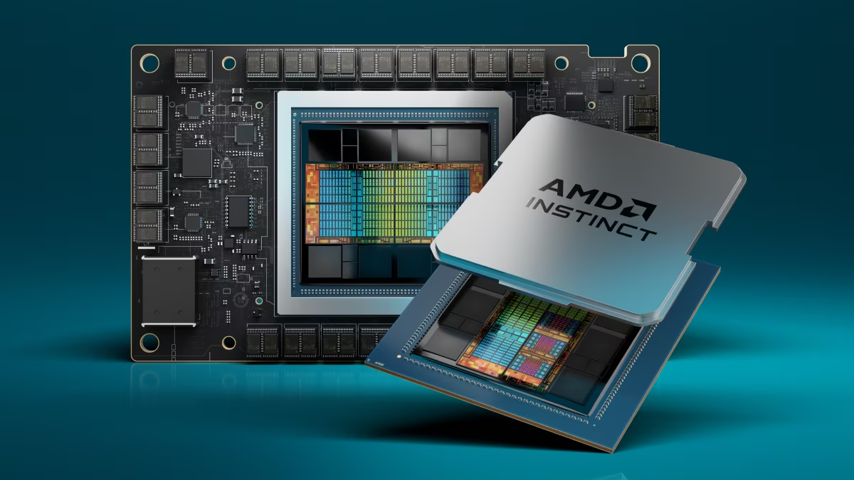
1. AMD Instinct MI300 Series Accelerators
The AMD Instinct™ MI300 Series Accelerators are the pillars of AI and HPC (High-Performance Computing). With a strong architecture and capabilities, these accelerators can tackle demanding workloads. Powered by the AMD CDNA™ 3 architecture, they offer compute performance, memory density, and high-bandwidth memory.
Benefits and Applications AMD Instinct MI300
- Supercharging AI and HPC: Exceptional compute performance, large memory density, and support for specialized data formats.
- Energy Efficiency: Efficient utilization of resources for energy-saving operations.
- Scalability: Scalable architecture for seamless integration and deployment in various environments.
- Accelerating Time-to-Market: Ready-to-deploy platforms reduce development costs and accelerate time-to-market.
- Advancing Exascale Computing: Powering supercomputers for groundbreaking simulations and scientific research.
- AI and HPC Workload Acceleration: Accelerating AI and HPC workloads pushes performance and efficiency boundaries.
| Feature | Description |
|---|---|
| CDNA™ 3 Architecture | Built on CDNA™ 3 architecture, it supports a wide range of precision capabilities. |
| Compute Units (CUs) | 304 GPU Compute Units for robust compute performance. |
| Memory | 192 GB HBM3 Memory for large memory density. |
| Peak Memory Bandwidth | 5.3 TB/s Peak Theoretical Memory Bandwidth for high-speed data processing. |
| Platform Integration | Integration of 8 MI300X GPU OAM modules for seamless deployment and scalability. |
| MI300A APUs Integration | Integration of 228 CUs and 24 "Zen 4" x86 CPU Cores for enhanced efficiency and flexibility. |
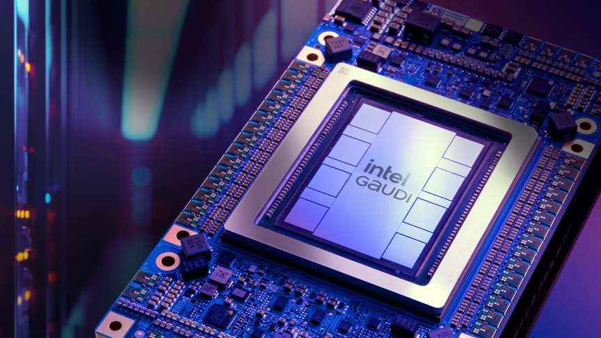
2. Intel Gaudi 3
Intel Gaudi 3 AI accelerator, introduced at the Intel Vision event in April 2024, is designed to address the generative AI gap. Offering performance, openness, and choice, Gaudi 3 leverages open community-based software to provide scalability for enterprise AI initiatives. It offers industry-standard Ethernet networking capabilities.
Benefits of Intel Gaudi 3
- Improved Performance: Intel Gaudi 3 is claimed to offer 50% faster time-to-train on average and 40% better power efficiency than competitors.
- Flexibility: Gaudi 3 enables enterprises to scale flexibly from single nodes to mega-clusters, supporting various AI tasks.
- Cost-Efficiency: Gaudi 3 delivers superior performance at a fraction of the cost, making it a cost-effective solution for enterprises.
- Open Community Software: The chip supports open community-based software, fostering collaboration and innovation in the AI ecosystem.
| Features | Description |
|---|---|
| Architecture | Intel Gaudi 3 is built on a sophisticated architecture, promising 4x more AI compute for BF16. |
| Compute Performance | The accelerator delivers exceptional AI training and inference performance, facilitating scalability. |
| Memory Bandwidth | Gaudi 3 boasts a 1.5x increase in memory bandwidth over its predecessor, ensuring efficient operations. |
| Ethernet Networking | Gaudi 3 supports industry-standard Ethernet networking, allowing enterprises to scale flexibly. |
3. Nvidia Blackwell B200
The NVIDIA Blackwell B200 is designed to deliver great performance for demanding workloads. It features an architecture that connects two NVIDIA B200 Tensor Core GPUs to the NVIDIA Grace CPU via an ultra-low-power NVLink chip-to-chip interconnect, enabling easy communication and optimized processing.
Benefits of NVIDIA Blackwell B200
- Enhanced Performance: Delivers great performance for compute-intensive AI workloads, offering up to 30x performance increase compared to previous GPU models.
- Cost and Energy Efficiency: Reduces cost and energy consumption by up to 25x, providing a more efficient solution for AI processing tasks.
- Scalability and Flexibility: Offers scalable solutions for enterprises that can link multiple Blackwell B200 chips in a rack-scale system, meeting diverse AI processing requirements.
- Cloud Availability and Integration: Accessible through major cloud service providers and supported by a wide network of cloud partners, ensuring seamless integration and deployment in cloud environments.
- Industry Collaboration: Supported by leading hardware and software companies, including Cisco, Dell, AWS, Google Cloud, and Microsoft Azure, fostering a robust ecosystem for AI development and deployment.
| Features | Description |
|---|---|
| Architecture | Connects two NVIDIA B200 Tensor Core GPUs to the NVIDIA Grace CPU via a 900GB/s NVLink interconnect. |
| Networking Platforms | Compatible with NVIDIA Quantum-X800 InfiniBand and Spectrum-X800 Ethernet platforms for high-speed networking. |
| System Integration | An integral component of the NVIDIA GB200 NVL72, a multi-node rack-scale system featuring 36 Grace Blackwell Superchips interconnected by fifth-generation NVLink. |
| Performance | Provides up to 30x performance increase compared to NVIDIA H100 Tensor Core GPUs for LLM inference workloads. |
| Memory | Offers a single GPU with 1.4 exaflops of AI performance and 30TB of fast memory. |
| Compatibility | Supported by NVIDIA HGX B200 server board, enabling linkage of eight B200 GPUs through NVLink. |
| Cloud Service Providers and Partnerships | Available through major cloud service providers such as AWS, Google Cloud, Microsoft Azure, and Oracle Cloud Infrastructure, as well as various cloud partners and sovereign AI clouds. |
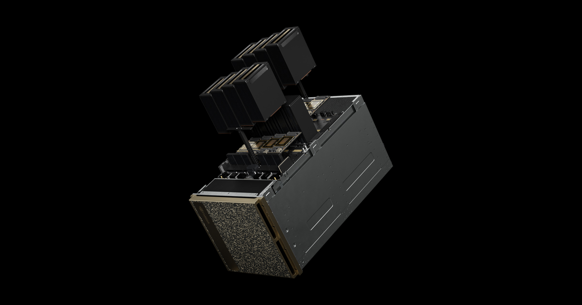
4. Cerebras Wafer Scale Engine 3 (WSE-3)
The Cerebras Wafer Scale Engine 3 is an advanced AI processor that revolutionizes computational performance. With 5 nm TSMC and 4000 transistors, it delivers exceptional capabilities for AI training tasks. The WSE-3 features an eight-wide FP16 SIMD math unit, a notable upgrade from the four-wide SIMD engine utilized in the WSE-1 and WSE-2 compute engines.
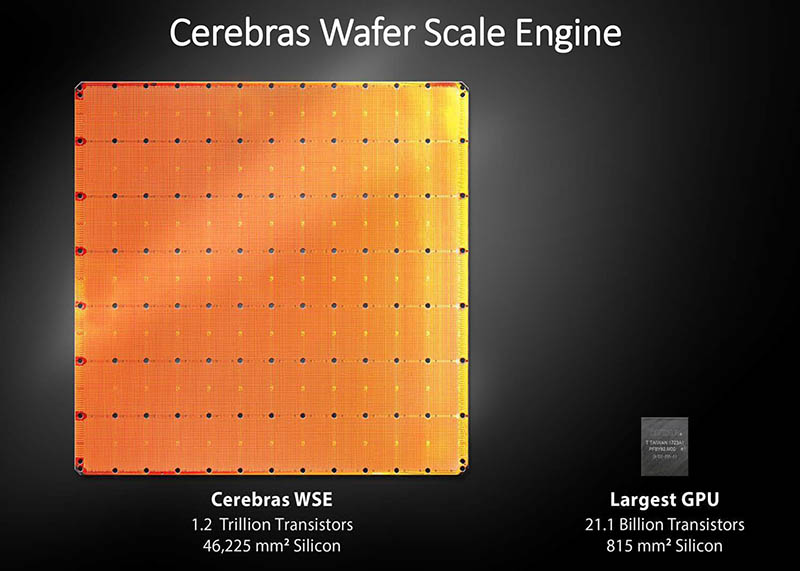
Benefits of Cerebras Wafer Scale Engine 3
- Enhanced Performance: Achieves a significant performance improvement, delivering twice the computational power compared to previous versions.
- Improved Memory Capacity: Offers expanded on-chip SRAM capacity, providing ample memory for data-intensive AI tasks.
- High Memory Bandwidth: The substantial SRAM bandwidth ensures rapid data access and processing, enhancing overall system performance.
- Scalability and Flexibility: Supports clustering of multiple systems, allowing for scalability to meet the diverse computational needs of enterprise and hyperscale environments.
- Cost-Effective AI Training: Provides an efficient solution for AI model training and is a cost-effective alternative to traditional GPU-based systems.
| Features | Description |
|---|---|
| Process Technology | Utilizes a 5-nanometer process technology, allowing for increased core density and improved clock speeds. |
| Matrix Math Engine | Enhanced eight-wide FP16 SIMD math unit, providing approximately 1.8 times more computational power. |
| On-Chip SRAM | Offers on-chip SRAM capacity of 44 GB, with a 10% increase compared to previous versions. |
| Memory Bandwidth | Provides an impressive SRAM bandwidth of 21 PB/sec per wafer, ensuring high-speed data access and processing. |
| Fabric Bandwidth | Despite a slight decrease, the fabric bandwidth allows significant performance gains. |
| Scalability and System Integration | Supports clustering of up to 2,048 systems, enabling a performance scale of up to 21.3 times compared to previous versions. |
5. Google TPU v5p
With a 2X price performance improvement over its predecessors, the Google TPU v5p powerhouse accelerator offers training capabilities and serves AI-powered applications like YouTube, Gmail, Google Maps, Google Play, and Android.
Comprising 8,960 chips in a pod configuration, the TPU v5p has the power of a high-bandwidth inter-chip interconnect (ICI) at a 4,800 Gbps/chip, facilitating lightning-fast data processing.
Benefits of Google TPU v5p
- Improved Performance: 2.8X LLM training speed improved compared to its predecessor, TPU v4.
- Enhanced Scalability: 4X more scalability in total available FLOPs per pod.
- Faster Training of AI Models: Train large foundation models, allowing for rapid experimentation and iteration in AI research.
- Seamless Transition: User-friendly JAX framework for smooth integration.
- Support for ML Frameworks: Extensive support for popular ML frameworks such as JAX, TensorFlow, and PyTorch, ensuring compatibility with existing workflows.
- Robust Orchestration Tools: Features open and unique Multislice Training and Multihost Inferencing software, optimizing resource utilization.
| Feature | Description |
|---|---|
| Number of chips per pod | 8,960 chips per pod, the TPU v5p offers immense computational power. |
| Inter-chip interconnect (ICI) | Ultra-high inter-chip interconnect speed of 4,800 Gbps/chip for data transfer. |
| Floating-point operations (FLOPS) | Delivers more than 2X the floating-point operations compared to its predecessor, TPU v4. |
| High-bandwidth memory (HBM) | 3X higher bandwidth memory than TPU v4. |
| SparseCores | Second-generation SparseCores accelerates training for embedding-dense models. |
Factors to Consider When Choosing an AI Chip
When selecting an AI chip for your applications, several factors should be considered to ensure optimal compatibility with your infrastructure. These factors include:
1. Performance
Look for chips with high computational power capable of handling the tasks required by your AI applications. Assess metrics such as floating-point operations per second (FLOPS) and memory bandwidth to gauge performance levels accurately.
2. Energy Efficiency
Power consumption can significantly impact operational costs at large-scale deployments, so getting an energy-efficient option is crucial. Evaluate chips that balance performance and energy efficiency, allowing you to achieve high computational throughput while minimizing power consumption.
3. Scalability
Choose chips that can scale efficiently, whether horizontally by adding more chips to existing systems or vertically by upgrading to higher-performance models without disrupting operations.
4. Compatibility
Consider chips that support popular machine learning frameworks, programming languages, and development tools commonly used in your organization. Additionally, ensure compatibility with your existing hardware architecture and data processing pipelines to avoid issues.
Future of AI Chips
One prominent trend shaping the future of AI chips is the integration of specialized hardware accelerators optimized for specific AI tasks, such as neural network inference and training. These accelerators, including tensor processing units (TPUs), field-programmable gate arrays (FPGAs), and application-specific integrated circuits (ASICs), offer energy efficiency for AI workloads.
The expansion of advanced AI chips holds the potential to revolutionize various industries by accelerating the development and deployment of AI. Organizations can train and run sophisticated AI models at scale with faster and more energy-efficient chips, unlocking new capabilities in natural language processing, computer vision, autonomous systems, and healthcare.


